
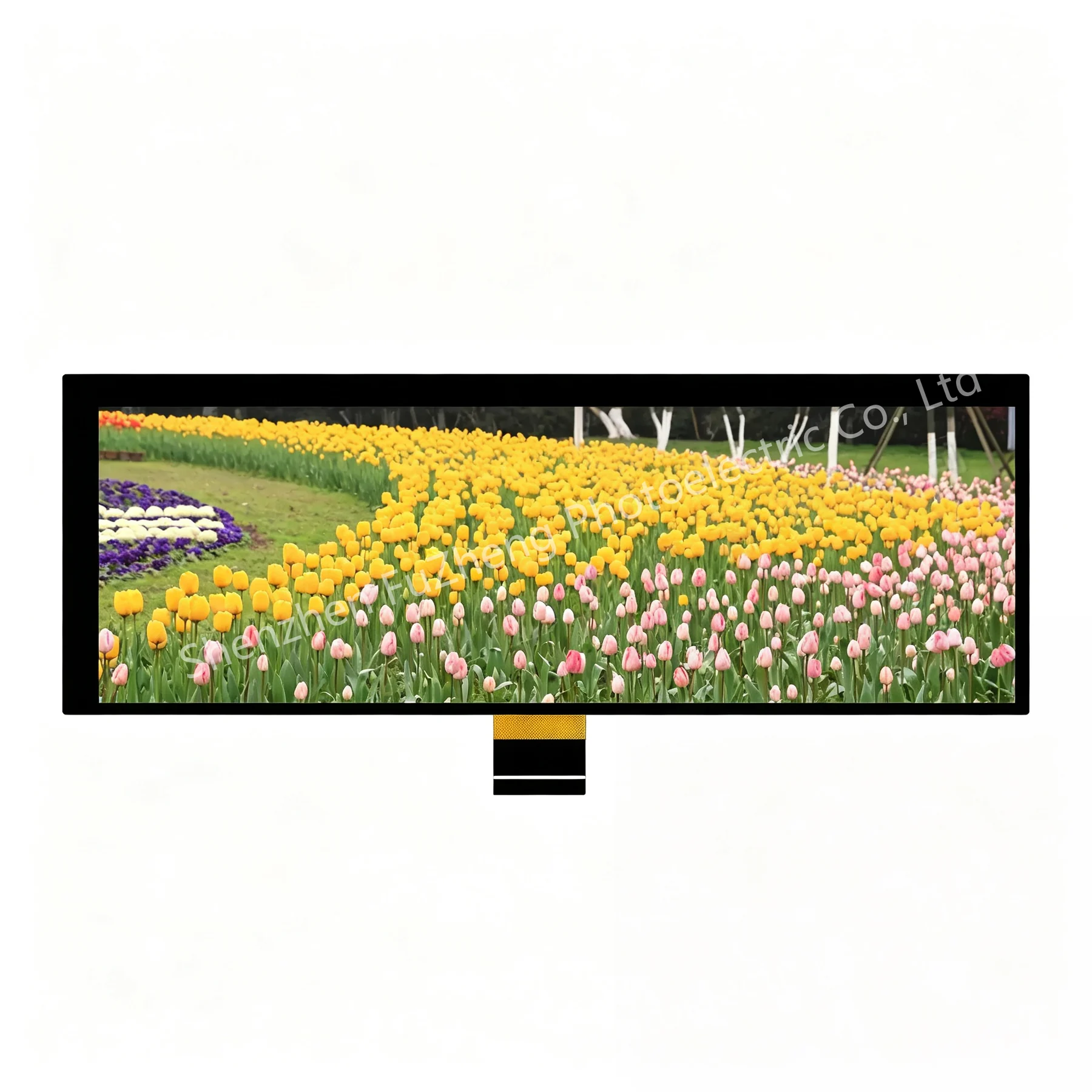
Images belong to this source record. Confirm the selected assembly and drawing revision before design-in.
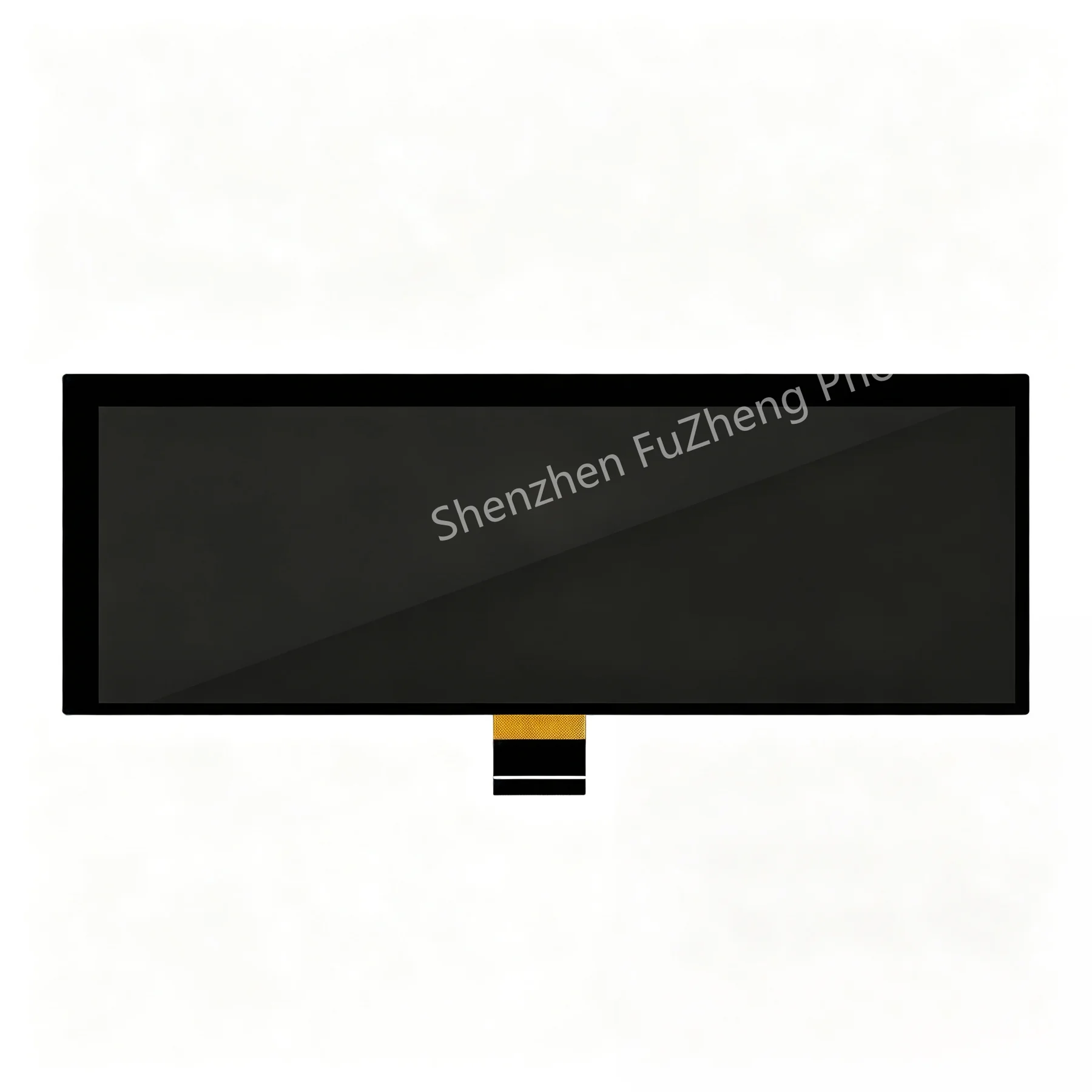
Model no.FZ81600C40
8 inch 1600x480 Ultra-Wide Bar-Type IPS LVDS TFT-LCD — FZ81600C40 (40-pin, HX8249+HX8678)
FZ81600C40 — 8 inch 1600x480 ultra-wide bar-type IPS LVDS TFT-LCD, 40-pin, HX8249+HX8678 driver. 204.5x70x1.0 mm slim strip form factor. Ideal for shelf label, queue display, EV charging, smart home. Factory price, OEM/ODM.
- a-Si TFT
- LVDS Interface
- No touch
- 8 inch a-Si TFT, 1600x480 ultra-wide bar (10:3 aspect), 16.7M colors
- Ultra-slim bar form factor: 204.5 x 70 x 1.0 mm — fits in shelf edges and narrow bezels
- Himax HX8249 (source) + HX8678 (gate) dual-chip driver — industry-proven
- IPS panel with All-direction full viewing angle
- Standard LVDS interface (4 data lanes + 1 clock lane)
- Screen Size
- 8 inch
- Resolution
- 1600 × 480
- Technology
- a-Si TFT
- Interface
- LVDS
- Touch
- No touch panel
- Viewing Angle
- IPS, full viewing angle
Product Overview
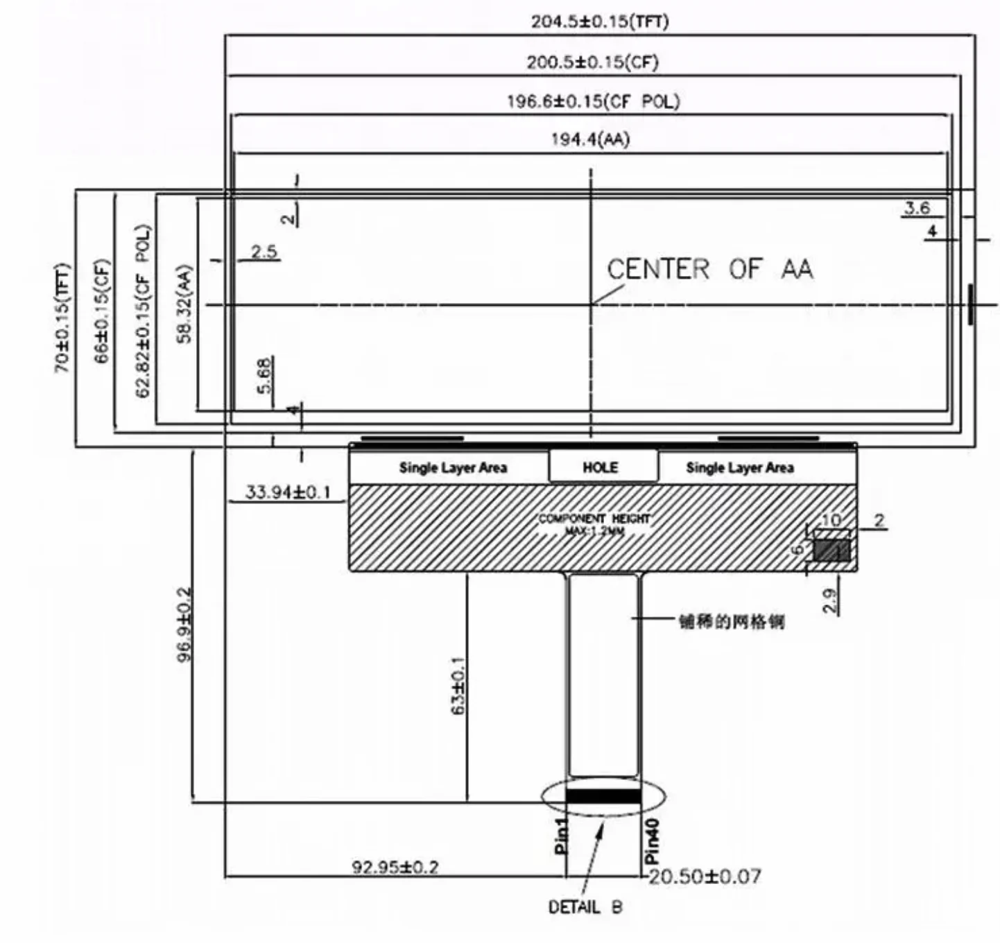
The FZ81600C40 is an 8″ ultra-wide bar-type IPS TFT-LCD module with 1600x480 resolution (10:3 aspect ratio) in a remarkably slim 204.5 (W) x 70 (H) x 1.0 (D) mm — ultra-slim bar form factor outline — only 70 mm tall and 1.0 mm thick. It uses a standard LVDS interface on a 40-pin plug-in FPC and is driven by the industry-proven Himax HX8249 + HX8678 dual-chip solution. The full-direction viewing angle, 16.7M color depth and 6/8-bit mode selection provide flexible integration with most industrial video controllers. The RL and TB mirror pins enable easy image inversion for top-mount or bottom-mount installations. Ideal for shelf-edge price labels, queue / status displays, EV charging status, smart-home control bars, factory production-line indicators, vehicle dashboard and any application where a wide, narrow strip display is required.
Key Features
- 8 inch a-Si TFT, 1600x480 ultra-wide bar (10:3 aspect), 16.7M colors
- Ultra-slim bar form factor: 204.5 x 70 x 1.0 mm — fits in shelf edges and narrow bezels
- Himax HX8249 (source) + HX8678 (gate) dual-chip driver — industry-proven
- IPS panel with All-direction full viewing angle
- Standard LVDS interface (4 data lanes + 1 clock lane)
- RL / TB mirror pins (Pin 30/31) — flexible image inversion
- 6-bit / 8-bit mode selectable via SELB (Pin 5) — compatible with older hosts
- Operating temperature -20 ~ +70 °C, storage -30 ~ +80 °C
Product Images
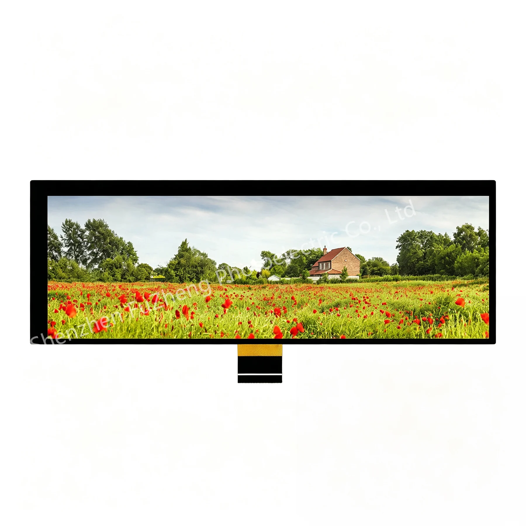
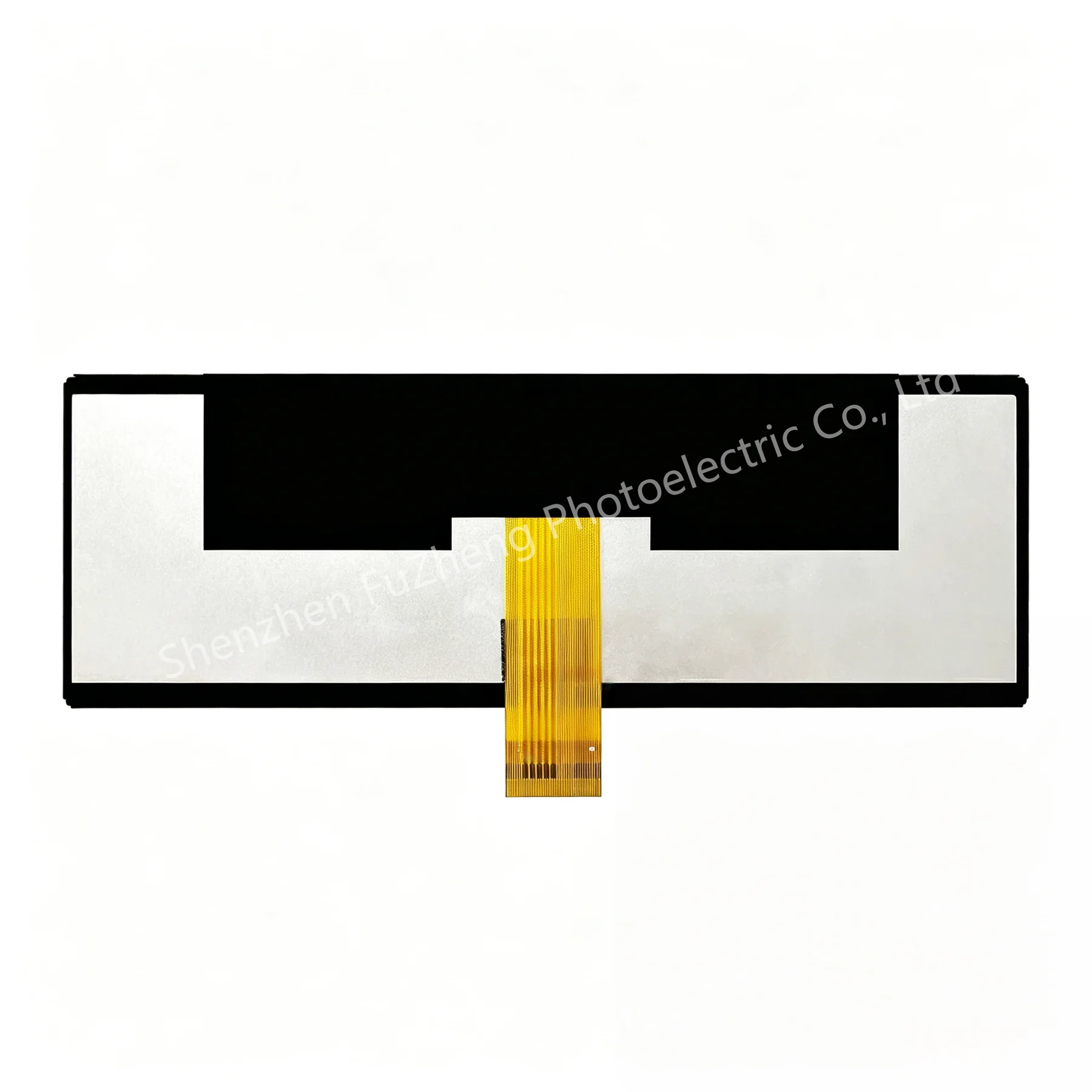
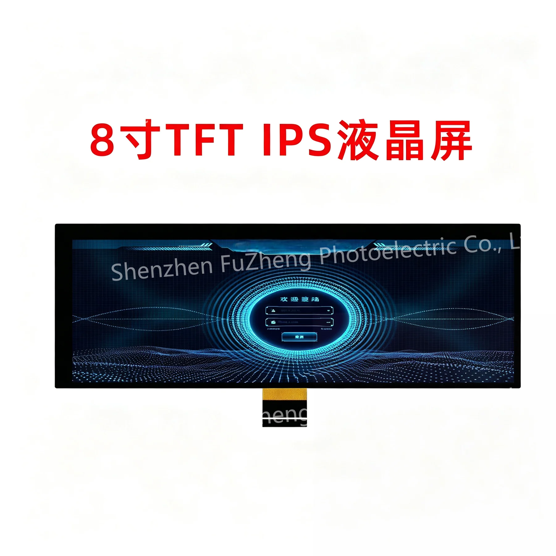
Basic Parameters
| Display Type | a-Si TFT |
|---|---|
| Model Number | FZ81600C40 |
| Screen Size | 8 inch (diagonal, ultra-wide bar / strip form factor) |
| Resolution | 1600x480 (1600 RGB x 480 Dots, 10:3 aspect) |
| Pixel Pitch (true) | 0.0934 (W) x 0.1215 (H) mm (149.4/1600 = 0.0934, 58.32/480 = 0.1215) |
| Display Colors | 16.7M (RGB 8-bit / 6-bit selectable via Pin 5 SELB) |
| Viewing Direction | IPS — All-direction (full viewing angle) |
| Active Area | 149.4 (W) x 58.32 (H) mm |
| LCM Outline Size | 204.5 (W) x 70 (H) x 1.0 (D) mm — ultra-slim bar form factor |
| Form Factor | Bar / Strip form factor — ideal for shelf edge, status display, queue, signage |
| Data Interface | LVDS Interface |
| Pin Count | 40 (plug-in FPC) |
| Controller / Driver IC | HX8249 (source driver) + HX8678 (gate driver) — Himax dual-chip solution |
| Image Mirror | Yes — RL horizontal shift direction (Pin 30), TB vertical shift direction (Pin 31) |
| Power Supply — VDD (Pin 3-4, digital) | VDD 2.8 ~ 3.5 V (Pin 3-4, digital circuit, +3.3 V typ. / 50 mA max) |
| Power Supply — VSDP (Pin 26-28, source +) | VSDP +5.5 V (Pin 26-28, source driver power, 80 mA max) |
| Power Supply — VSDN (Pin 23-25, source -) | VSDN -5.5 V (Pin 23-25, source driver negative supply, 80 mA max) |
| Power Supply — VDD_OTP (Pin 36, OTP only) | VDD_OTP 7.5 V (Pin 36, OTP programming only — leave NC for normal operation) |
| Touch Panel | No touch |
| Operating Temperature | -20 ~ +70 °C |
| Storage Temperature | -30 ~ +80 °C |
| Manufacturer | Shenzhen FuZheng Photoelectric Co., Ltd |
Mechanical Drawings
Pin Definition (40-pin FPC)
40-pin plug-in FPC tail. Pin 1 is STBYB (enable IC, normally pulled high). Pin 2 is active-low reset. Pins 3-4 are VDD (+3.3 V digital, 50 mA max). Pin 5 is SELB (6/8 bit mode). Pins 6-7 are GND. Pins 8-9 are LVDS Lane 0 differential pair (RXIN0-/+). Pin 10 is GND. Pins 11-12 are Lane 1 (RXIN1-/+). Pin 13 is GND. Pins 14-15 are LVDS clock pair (RXCLKIN-/+). Pin 16 is GND. Pins 17-18 are Lane 2 (RXIN2-/+). Pin 19 is GND. Pins 20-21 are Lane 3 (RXIN3-/+). Pin 22 is GND. Pins 23-25 are VSDN (-5.5 V, 80 mA max). Pins 26-28 are VSDP (+5.5 V, 80 mA max). Pin 29 is GND. Pin 30 is RL (horizontal shift). Pin 31 is TB (vertical shift). Pin 32 is ATREN (OTP only, leave NC). Pins 33-35 are CSB / SCL / SDA (SPI, OTP only). Pin 36 is VDD_OTP 7.5 V (OTP only, leave NC). Pins 37-38 are LED- (cathode). Pins 39-40 are LED+ (anode).
| Pin No. | Symbol | I/O | Description |
|---|---|---|---|
| 1 | STBYB | I | Enable IC (standby, normally pulled high) — Note 2 |
| 2 | Reset | I | Reset IC (active low) |
| 3 | VDD | P | Digital power +3.3 V (50 mA max) |
| 4 | VDD | P | Digital power +3.3 V (50 mA max) |
| 5 | SELB | I | 6bit / 8bit mode select — Note 4 |
| 6 | GND | P | Ground |
| 7 | GND | P | Ground |
| 8 | RXIN0- | I | Negative LVDS differential data input (Lane 0-) — PAD on bottom, pin 1 on right (top view); LVDS pair will not cross each other |
| 9 | RXIN0+ | I | Positive LVDS differential data input (Lane 0+) |
| 10 | GND | P | Ground |
| 11 | RXIN1- | I | Negative LVDS differential data input (Lane 1-) |
| 12 | RXIN1+ | I | Positive LVDS differential data input (Lane 1+) |
| 13 | GND | P | Ground |
| 14 | RXCLKIN- | I | Negative LVDS differential clock input |
| 15 | RXCLKIN+ | I | Positive LVDS differential clock input |
| 16 | GND | P | Ground |
| 17 | RXIN2- | I | Negative LVDS differential data input (Lane 2-) |
| 18 | RXIN2+ | I | Positive LVDS differential data input (Lane 2+) |
| 19 | GND | P | Ground |
| 20 | RXIN3- | I | Negative LVDS differential data input (Lane 3-) |
| 21 | RXIN3+ | I | Positive LVDS differential data input (Lane 3+) |
| 22 | GND | P | Ground |
| 23 | VSDN | P | Power for Driver IC (negative supply -5.5 V, 80 mA max) |
| 24 | VSDN | P | Power for Driver IC (negative supply -5.5 V, 80 mA max) |
| 25 | VSDN | P | Power for Driver IC (negative supply -5.5 V, 80 mA max) |
| 26 | VSDP | P | Power for Driver IC (positive supply +5.5 V, 80 mA max) |
| 27 | VSDP | P | Power for Driver IC (positive supply +5.5 V, 80 mA max) |
| 28 | VSDP | P | Power for Driver IC (positive supply +5.5 V, 80 mA max) |
| 29 | GND | P | Ground |
| 30 | RL | I | Horizontal shift direction (left/right mirror) — Note 5 |
| 31 | TB | I | Vertical shift direction (up/down mirror) — Note 5 |
| 32 | ATREN | I | Only for OTP program (leave NC for normal operation) |
| 33 | CSB | - | SPI chip select (for OTP programming only) |
| 34 | SCL | - | SPI clock (for OTP programming only) |
| 35 | SDA | - | SPI data (for OTP programming only) |
| 36 | VDD_OTP | P | 7.5 V for OTP program (leave NC for normal operation) |
| 37 | LED- | P | LED cathode (backlight) |
| 38 | LED- | P | LED cathode (backlight) |
| 39 | LED+ | P | LED anode (backlight) |
| 40 | LED+ | P | LED anode (backlight) |
Power Supply Requirements
Three independent power rails are required: VDD +3.3 V digital (Pin 3-4, 50 mA max), VSDP +5.5 V source-driver positive supply (Pin 26-28, 80 mA max), and VSDN -5.5 V source-driver negative supply (Pin 23-25, 80 mA max). VDD_OTP 7.5 V (Pin 36) is for factory OTP programming only — leave NC for normal operation. The ATREN / CSB / SCL / SDA pins (32-35) are also for OTP programming only.
Typical Applications
- Retail shelf-edge price label and electronic shelf label (ESL) display
- Queue / waiting-number display and bank / hospital status indicator
- EV charging station status display and parking guidance sign
- Smart home control bar and home automation status display
- Factory production-line indicator and assembly-line status panel
- Vehicle dashboard secondary display, taxi-top advertisement display
- Public transportation information strip (bus / metro arrival, gate display)
- Conference room room-status display and meeting-schedule strip
Frequently Asked Questions
What are the size and resolution of FZ81600C40?
FZ81600C40 is a 8 inch (diagonal, ultra-wide bar / strip form factor) display with 1600x480 (1600 RGB x 480 Dots, 10:3 aspect).
Which interface and connector does FZ81600C40 use?
The supplied product brief specifies LVDS Interface with 40 (plug-in FPC). Confirm the quoted connector revision before design-in.
Which controller or driver is used on FZ81600C40?
The supplied record identifies HX8249 (source driver) + HX8678 (gate driver) — Himax dual-chip solution. Initialization and timing data should be confirmed against the approved revision.
What are the outline and viewing characteristics of FZ81600C40?
The published module outline is 204.5 (W) x 70 (H) x 1.0 (D) mm — ultra-slim bar form factor, and the viewing specification is IPS — All-direction (full viewing angle).
What operating temperature is specified for FZ81600C40?
The supplied product brief lists an operating temperature of -20 ~ +70 °C. OEM/ODM options should be confirmed during quotation.
Ordering & Contact
Sample orders and OEM/ODM quotations are available. Please contact Shenzhen FuZheng Photoelectric Co., Ltd by email or WhatsApp.
Contact: Victory.Wang | Shenzhen FuZheng Photoelectric Co., Ltd | Email: Victory.Wang@szfuzheng.com | WhatsApp: +86 15989445783 | Website: https://fzlcddisplay.com
Compare more in Bar Type TFT Displays.
1.99-Inch 170x320 Bar TFT-LCD Display
Explore the 1.99-Inch 170x320 Bar TFT-LCD Display, a IPS TFT-LCD panel, with source-backed images and published specifications. Request a sample or engineering RFQ.

23.6-Inch Bar Type TFT-LCD Display Module
Explore the 23.6-Inch Bar Type TFT-LCD Display Module, with source-backed images and published specifications. Request a sample or engineering RFQ.
28.6 inch Bar type TFT display
Explore the 28.6 inch Bar type TFT display, a TFT-LCD display module, with source-backed images and published specifications. Request a sample or engineering RFQ.
Discuss this display with our team
FZ81600C40
Share the required interface, touch assembly, quantity and project timing. Pricing and availability are confirmed by inquiry.